- 您现在的位置:买卖IC网 > Sheet目录493 > NTTFS4939NTAG (ON Semiconductor)MOSFET N-CH 30V 8.9A 8WDFN
�� �
�
�NTTFS4939N�
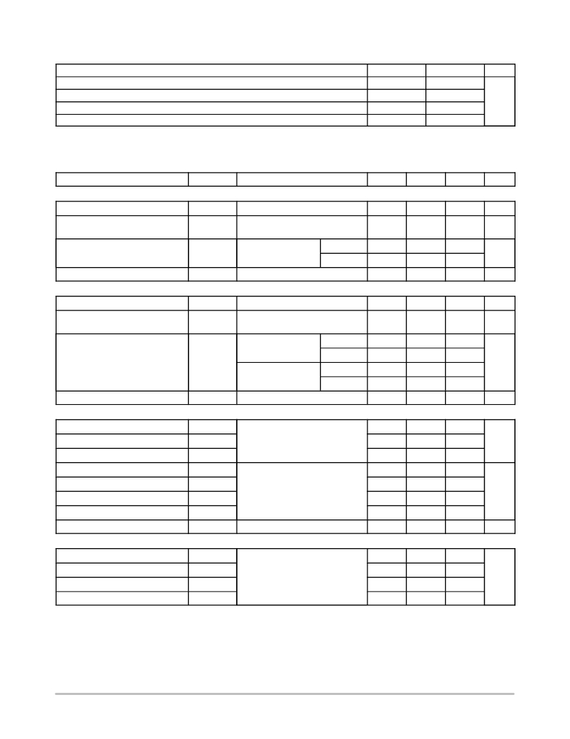
�THERMAL� RESISTANCE� MAXIMUM� RATINGS�
�Parameter�
�Junction� ?� to� ?� Case� (Drain)�
�Junction� ?� to� ?� Ambient� –� Steady� State� (Note� 3)�
�Junction� ?� to� ?� Ambient� –� Steady� State� (Note� 4)�
�Junction� ?� to� ?� Ambient� –� (t� ≤� 10� s)� (Note� 3)�
�Symbol�
�R� q� JC�
�R� q� JA�
�R� q� JA�
�R� q� JA�
�Value�
�4.2�
�56.5�
�146.5�
�28�
�Unit�
�°� C/W�
�3.� Surface� ?� mounted� on� FR4� board� using� 1� sq� ?� in� pad,� 1� oz� Cu.�
�4.� Surface� ?� mounted� on� FR4� board� using� the� minimum� recommended� pad� size� (40� mm� 2� ,� 1� oz.� Cu).�
�ELECTRICAL� CHARACTERISTICS� (T� J� =� 25� °� C� unless� otherwise� specified)�
�Parameter�
�Symbol�
�Test� Condition�
�Min�
�Typ�
�Max�
�Unit�
�OFF� CHARACTERISTICS�
�Drain� ?� to� ?� Source� Breakdown� Voltage�
�Drain� ?� to� ?� Source� Breakdown� Voltage�
�Temperature� Coefficient�
�V� (BR)DSS�
�V� (BR)DSS� /T� J�
�V� GS� =� 0� V,� I� D� =� 250� m� A�
�30�
�15�
�V�
�mV/� °� C�
�Zero� Gate� Voltage� Drain� Current�
�I� DSS�
�V� GS� =� 0� V,�
�V� DS� =� 24� V�
�T� J� =� 25� °� C�
�T� J� =� 125� °� C�
�1.0�
�10�
�m� A�
�Gate� ?� to� ?� Source� Leakage� Current�
�I� GSS�
�V� DS� =� 0� V,� V� GS� =� ±� 20� V�
�±� 100�
�nA�
�ON� CHARACTERISTICS� (Note� 5)�
�Gate� Threshold� Voltage�
�Negative� Threshold� Temperature�
�Coefficient�
�V� GS(TH)�
�V� GS(TH)� /T� J�
�V� GS� =� V� DS� ,� I� D� =� 250� m� A�
�1.2�
�4.0�
�2.2�
�V�
�mV/� °� C�
�Drain� ?� to� ?� Source� On� Resistance�
�R� DS(on)�
�V� GS� =� 10� V�
�I� D� =� 20� A�
�I� D� =� 10� A�
�4.1�
�4.1�
�5.5�
�m� W�
�V� GS� =� 4.5� V�
�I� D� =� 20� A�
�I� D� =� 10� A�
�6.0�
�5.9�
�8.0�
�Forward� Transconductance�
�g� FS�
�V� DS� =� 1.5� V,� I� D� =� 15� A�
�35�
�S�
�CHARGES� AND� CAPACITANCES�
�Input� Capacitance�
�C� iss�
�1979�
�pF�
�Output� Capacitance�
�Reverse� Transfer� Capacitance�
�C� oss�
�C� rss�
�V� GS� =� 0� V,� f� =� 1.0� MHz,� V� DS� =� 15� V�
�711�
�20.2�
�Total� Gate� Charge�
�Q� G(TOT)�
�12.4�
�nC�
�Threshold� Gate� Charge�
�Gate� ?� to� ?� Source� Charge�
�Gate� ?� to� ?� Drain� Charge�
�Q� G(TH)�
�Q� GS�
�Q� GD�
�V� GS� =� 4.5� V,� V� DS� =� 15� V,� I� D� =� 20� A�
�3.2�
�6.0�
�1.8�
�Total� Gate� Charge�
�Q� G(TOT)�
�V� GS� =� 10� V,� V� DS� =� 15� V,� I� D� =� 20� A�
�28�
�nC�
�SWITCHING� CHARACTERISTICS� (Note� 6)�
�Turn� ?� On� Delay� Time�
�t� d(on)�
�12.2�
�ns�
�Rise� Time�
�Turn� ?� Off� Delay� Time�
�Fall� Time�
�t� r�
�t� d(off)�
�t� f�
�V� GS� =� 4.5� V,� V� DS� =� 15� V,�
�I� D� =� 15� A,� R� G� =� 3.0� W�
�20.6�
�20.8�
�3.9�
�5.� Pulse� Test:� pulse� width� =� 300� m� s,� duty� cycle� v� 2%.�
�6.� Switching� characteristics� are� independent� of� operating� junction� temperatures.�
�http://onsemi.com�
�2�
�发布紧急采购,3分钟左右您将得到回复。
相关PDF资料
NTTFS4941NTAG
MOSFET N-CH 30V 8.3A 8WDFN
NTTFS4985NFTAG
MOSFET N-CH 30V 16.3A 8-WDFN
NTTFS5116PLTAG
MOSFET PWR P-CH 60V 5.7A 8-WDFN
NTTFS5811NLTWG
MOSFET N-CH 40V 53.6A 8DFN
NTTFS5820NLTWG
MOSFET N-CH 60V 37A 8DFN
NTTFS5826NLTWG
MOSFET PWR N-CH 60V 20A 8-WDFN
NTTS2P02R2
MOSFET P-CH 20V 2.4A 8MICRO
NTTS2P03R2
MOSFET P-CH 30V 2.1A 8MICRO
相关代理商/技术参数
NTTFS4939NTWG
功能描述:MOSFET 30V 56A 5.5 mOhm Single N-Chan u8FL RoHS:否 制造商:STMicroelectronics 晶体管极性:N-Channel 汲极/源极击穿电压:650 V 闸/源击穿电压:25 V 漏极连续电流:130 A 电阻汲极/源极 RDS(导通):0.014 Ohms 配置:Single 最大工作温度: 安装风格:Through Hole 封装 / 箱体:Max247 封装:Tube
NTTFS4941N
制造商:ONSEMI 制造商全称:ON Semiconductor 功能描述:Power MOSFET 30 V, 46 A, Single N−Channel, μ8FL
NTTFS4941NTAG
功能描述:MOSFET 30V 46A 6.2 mOhm Single N-Chan u8FL RoHS:否 制造商:STMicroelectronics 晶体管极性:N-Channel 汲极/源极击穿电压:650 V 闸/源击穿电压:25 V 漏极连续电流:130 A 电阻汲极/源极 RDS(导通):0.014 Ohms 配置:Single 最大工作温度: 安装风格:Through Hole 封装 / 箱体:Max247 封装:Tube
NTTFS4941NTWG
功能描述:MOSFET 30V 46A 6.2 mOhm Single N-Chan u8FL RoHS:否 制造商:STMicroelectronics 晶体管极性:N-Channel 汲极/源极击穿电压:650 V 闸/源击穿电压:25 V 漏极连续电流:130 A 电阻汲极/源极 RDS(导通):0.014 Ohms 配置:Single 最大工作温度: 安装风格:Through Hole 封装 / 箱体:Max247 封装:Tube
NTTFS4943N
制造商:ONSEMI 制造商全称:ON Semiconductor 功能描述:Power MOSFET 30 V, 41 A, Single N−Channel, μ8FL
NTTFS4943NTAG
功能描述:MOSFET 30V 41A 7.2 mOhm Single N-Chan u8FL RoHS:否 制造商:STMicroelectronics 晶体管极性:N-Channel 汲极/源极击穿电压:650 V 闸/源击穿电压:25 V 漏极连续电流:130 A 电阻汲极/源极 RDS(导通):0.014 Ohms 配置:Single 最大工作温度: 安装风格:Through Hole 封装 / 箱体:Max247 封装:Tube
NTTFS4943NTWG
功能描述:MOSFET 30V 41A 7.2 mOhm Single N-Chan u8FL RoHS:否 制造商:STMicroelectronics 晶体管极性:N-Channel 汲极/源极击穿电压:650 V 闸/源击穿电压:25 V 漏极连续电流:130 A 电阻汲极/源极 RDS(导通):0.014 Ohms 配置:Single 最大工作温度: 安装风格:Through Hole 封装 / 箱体:Max247 封装:Tube
NTTFS4945N
制造商:ONSEMI 制造商全称:ON Semiconductor 功能描述:Power MOSFET 30 V, 34 A, Single N−Channel, μ8FL